|
|
CopyrightCopyright (c) 1997 by Brand Innovators of Digital Products bv. All rights reserved. No part of this publication may be reproduced, transmitted, transcribed, stored in a retrieval system, or translated into any language or computer language, in any form or by any means, electronic, mechanical, magnetic, optical, chemical, manual or otherwise, without the prior written permission of Brand Innovators of Digital Products bv, Post Office Box 1377, 5602 BJ Eindhoven - The Netherlands. DisclaimerThe information in this document has been carefully checked and is believed to be entirely reliable. However, no responsibility is assumed for inaccuracies. Brand Innovators of Digital Products bv makes no representations or warranties with respect to the contents hereof and specifically disclaims any implied warranties of merchant ability or fitness for any particular purpose. Furthermore, Brand Innovators of Digital Products bv reserves the right to make changes to any product herein to improve reliability, function or design, without obligation of Brand Innovators of Digital Products bv to notify any person of such revision or changes. Brand Innovators of Digital Products bv does not assume any liability arising out of applications or use of any product or circuit described herein; neither does it convey any license under its patent rights nor the rights of others. Chapter 1 General Information 1-1Chapter 2 Specifications 2-1Chapter 3 Installation Procedures 3-13.7 CAN Channel Connection 3-3 3.11 Power Supply Connection 3-4 Chapter 4 Functional Description 4-14.3.1 Differences in the Companion Mode 4-1 4.5.1 Power Supply Monitor Reset 4-2 4.5.2 Hardware Watchdog Circuit Reset 4-2 4.6 Serial Peripheral Interface 4-2 Chapter 5 Programming Considerations 5-15.2 Register Settings for 68360 Master Mode 5-1 5.2.1 Module Base Address Register 5-1 5.2.2 Module Configuration Register 5-1 5.2.3 Auto Vector Register 5-1 5.2.4 Reset Status Register 5-2 5.2.5 CLKO Control Register 5-2 5.2.6 PLL Control Register 5-2 5.2.7 Port E Pin Assignment Register 5-2 5.2.8 System Protection Control 5-2 5.2.9 Global Memory Register 5-2 5.2.10 Base Register 0 and Option Register 0 5-3 5.2.11 Base Register 1 and Option Register 1 5-3 5.2.12 Base Register 2 and Option Register 2 5-3 5.2.13 Base Register 3 and Option Register 3 5-3 5.2.14 Base Register 4 and Option Register 4 5-3 5.2.15 Base Register 5 and Option Register 5 5-4 5.2.16 Base Register 6 and Option Register 6 5-4 5.2.17 Base Register 7 and Option Register 7 5-4 5.2.19 Port A Open Drain Register 5-5 5.2.20 Port A Data Register 5-5 5.2.21 Port A Data Direction Register 5-5 5.2.22 Port A Pin Assignment Register 5-5 5.2.24 Port B Open Drain Register 5-6 5.2.25 Port B Data Register 5-6 5.2.26 Port B Data Direction Register 5-6 5.2.27 Port B Pin Assignment Register 5-6 5.2.29 Port C Data Register 5-7 5.2.30 Port C Data Direction Register 5-7 5.2.31 Port C Pin Assignment Register 5-7 5.2.32 Port C Special Options Register 5-7 5.3 Register Settings for Companion Mode 5-7 5.3.1 Module Base Address Register 5-7 5.3.2 Module Configuration Register 5-7 5.3.3 CLKO Control Register 5-8 5.3.4 PLL Control Register 5-8 5.3.5 Port E Pin Assignment Register 5-8 5.3.6 System Protection Control 5-8 5.3.7 Global Memory Register 5-8 5.3.8 Base Register 0 and Option Register 0 5-8 5.3.9 Base Register 1 and Option Register 1 5-8 5.3.10 Base Register 2 and Option Register 2 5-8 5.3.11 Base Register 3 and Option Register 3 5-8 5.3.12 Base Register 4 and Option Register 4 5-8 5.3.13 Base Register 5 and Option Register 5 5-8 5.3.14 Base Register 6 and Option Register 6 5-9 5.3.15 Base Register 7 and Option Register 7 5-9 5.4.5 Board Status Register 5-11 5.4.11 Temperature Sensor 5-14 5.4.12 Flex Configuration 5-14 5.5.2 Ethernet status LEDs 5-16 5.5.3 Processor Status LED 5-16 5.5.4 Power Indication LED 5-16 Appendix B Schematic Diagrams B-1 Appendix C Component Layout C-1 Appendix D List of Components D-1 Appendix E Connector Assignments E-1 Appendix G Mechanical Specifications G-1 Appendix H Application Notes H-1 Figure 5-1 Flex Configuration Timing 5-14Figure C-1 Component Layout C-1 Figure C-2 Jumper Locations C-2 Figure G-1 Mechanical Specifications G-1 Table 1-2 Ordering Information 1-2 Table 1-3 List of Documents 1-3 Table 3-1 Default Jumper Settings 3-1 Table 3-2 Slope Control Jumpers 3-2 Table 3-3 Watch Dog Enable 3-2 Table 3-4 Push Button Reset 3-2 Table 3-5 DRAM Access Times 3-3 Table 4-1 Devices on the SPI 4-2 Table 4-3 External Interrupt Sources 4-4 Table 5-1 MC68360 Port A Usage 5-4 Table 5-2 MC68360 Port B Usage 5-5 Table 5-3 MC68360 Port C Usage 5-6 Table 5-5 CAN Channel Configuration Register 5-10 Table 5-6 Board Status Register Usage 5-11 Table 5-7 CAN Channel Status 5-12 Table 5-8 Ethernet Control Signals 5-12 Table 5-9 RS-232 Modem Control Signals 5-12 Table 5-10 RS-485 Direction Control Signal 5-13 Table 5-11 Serial EEPROM Control Signals 5-13 Table 5-12 Real Time Clock Control Signals 5-13 Table 5-13 Temperature Sensor Control Signals 5-14 Table 5-14 Flex Configuration Timing 5-15 Table 5-15 Flex Configuration Control Signals 5-15 Table 5-16 CAN Channel LEDs 5-15 Table 5-17 Ethernet LED Indicators 5-16 Table 5-18 Processor Status 5-16 Table D-1 List of Capacitors D-1 Table D-2 List of Resistors D-1 Table D-3 List of Connectors and Jumpers D-1 Table D-4 List of Integrated Circuits D-2 Table D-5 List of Discrete Semiconductors D-3 Table D-6 List of Oscillators D-3 Table D-7 List of Miscellaneous Components D-3 Table E-2 10Base-T Connector E-1 Table E-3 Thin Coax Connector E-1 Table E-4 RS-232 Connector E-2 Table E-5 RS-485 Connector E-2 Table E-6 Power Supply Connector E-2 Table E-7 Boundary Scan Connector E-2 Table E-8 Background Debug Mode Connector E-3 Table E-9 DRAM SIMM-72 Pinning E-4 Table F-1 Cycle Types and Responding Devices F-1 Table F-2 Chip Select Assignments F-1 Table F-3 Addresses of CAN Channels F-2
| |||||||||||||||||||||||||||||||||||||||||||||||||||||||||||||||||||||||||||||||||||||||||||||||||||||||||||||||||||||||||||||||||||||||||||||||||||||||||||||||||||||||||||||||||||||||||||||||||||||||||||||||||||||||||||||||||||||||||||||||||||||||||||||||||||||||||||||||||||||||||||||||||||||||||||||||||||||||||||||||||||||||||||||||||||||||||||||||||||||||||||||||||||||||||||||||||||||||||||||||||||||||||||||||||||||||||||||||||||||||||||||||||||||||||||||||||||||||||||||||||||||||||||||||||||||||||||||||||||||||||||||||||||||||||||||||||||||||||||||||||||||||||||||||||||||||||||||||||||||||||||||||||||||||||||||||||||||||||||||||||||||||||||||||||||||||||||||||||||||||||||||||||||||||||||||||||||||||||||||||||||||||||||||||||||||||||||||||||||||||||||||||||||||||||||||||||||||||||||||||||||||||||||||||||||||||||||||||||||||||||||||||||||||||||||||||||||||||||||||||||||||||||||||||||||||||||||||||||||||||||||||||||||||||||||||||||||||||||||||||||||||||||||||||||||||||||||||||||||||||
|
The fault-tolerant CAN interface option was added, using the PCA82C252 CAN transceiver |
The next table gives an overview of the different options that are available for the BI-0501.
The following documentation can be referred to for detailed information about related items not described in this manual.
The BI-0501 is equipped with the SJA1000 CAN Controllers from Philips. The optical isolated physical interfaces are based on the PCA82C251 and the PCA82C252 CAN transceivers.
The following section gives an overview of the main parts that are used.
The MC68EN360 QUad Integrated Communication Controller (QUICC) is a versatile one chip integrated microprocessor and peripheral combination that can be used in a variety of controller applications. It particularly excels in communications activities. The QUICC (pronounced "quick") can be described as a next-generation MC68302 with higher performance in all areas of device operation, increased flexibility, major extensions in capability, and higher integration. The term "quad" comes from the fact there are four serial communication controllers (SCCs) on the device; however, there are actually seven serial channels: four SCCs, two serial management controllers (SMCs), and one serial peripheral interface (SPI).
Memory Controller supports DRAM, SRAM, EPROM, Flash EPROM.
RISC Communications Processor Module
The QUICC supports a slave mode to disable the internal CPU32+ which allows use with an external processor. The MC68040 Companion Mode allows the QUICC to be an MC68040 Companion Chip and intelligent peripheral. All the QUICC features are usable in the slave mode.
The MC68040 is Motorola's third generation of M68000-compatible, high performance, 32-bit microprocessors. The MC68040 is a virtual memory microprocessor employing multiple concurrent execution units and a highly integrated architecture that provides very high performance in a monolithic HCMOS device. The processor integrates an MC68030-compatible integer unit and two independent caches. It also contains dual, independent, demand-page memory management units (MMUs) for instruction and data stream accesses and independent, 4-KByte instruction and data caches. The MC68040 contains an MC68882-compatible floating-point unit (FPU). The use of multiple independent execution pipelines, multiple internal buses, and a full internal Harvard architecture, including separate physical caches for both instruction and data accesses, achieves a high degree of instruction execution parallelism.
The SJA1000 is a highly integrated stand-alone controller for the Controller Area Network (CAN) used within automotive and general industrial environments. It contains all the necessary features required to implement a high performance communication protocol. The programmable transfer rate of the SJA1000 goes up to 1 MBaud. The SJA1000 can operate in the BasicCAN (PCA82C200 compatible) and the PeliCAN (CAN 2.0B compatible) mode.
The PCA82C251 is the standard interface between the CAN protocol controller and the physical bus. It is intended for high speed applications up to 1 MBaud and is fully compatible with the ISO/DIS 11898 standard. The fault-tolerant option using the PCA82C252 transceiver is intended for low-speed applications with baud rates up to 125 kBaud. This option supports one-wire transmission in the event of bus failure.
The Flash memory consists of four 1-MBit or 4-MBit Flash type EPROMs, giving a 32-bit wide, 512 kByte or 2 MByte non-volatile execution memory. The Am29F040 is a 4 Mbit, 5.0 Volt-only Flash memory organized as 512 Kbyte of 8 bits each. This device can be programmed in-system with the standard system 5.0 V Vcc supply. This device also features a sector erase architecture. the sector mode allows for 64K byte blocks of memory to be erased and reprogrammed without effecting other blocks.
The SRAM memory consists of four 1-MBit type SRAMs, giving a 32-bit wide, 512 kByte data memory. The added DS1210 Nonvolatile Controller Chip converts the CMOS SRAM into nonvolatile memory.
The DRAM memory is located in a industry standard 72-pin SIMM socket giving 32-bit wide, 32 MByte of general purpose memory.
The 512 bytes serial E2PROM AT25040 is Serial Peripheral Interface (SPI) compatible and features a Write Disable instruction for software data protection.
The DS1620 Digital Thermometer provides 9-bit temperature readings which indicate the temperature of the device. User defined temperature settings are stored in nonvolatile memory. Temperature settings and readings are all communicated to and from the DS1620 over a 3-wire interface.
The DS1305 Serial Alarm Real Time Clock provides a full BCD clock calendar which is accessible via the SPI compatible serial interface. Two programmable time of day alarms are provided by the DS1305. Each alarm can generate an interrupt on a programmable combination of seconds, minutes, hours, and day.
Eight independent CAN channels
ISO/DIS 11898 compatible isolated physical interface
Front panel LED for each channel
Selects automatically the active interface
Asynchronous RS-232 with isolated physical interface
Fieldbus port RS-485 with isolated physical interface
The module is shipped in an antistatic container to protect the module against static electricity. When the module is unpacked, avoid touching areas of integrated circuitry to prevent static discharge from damaging the circuits.
Jumpers are used to select hardware specific options. The jumper block positioning and default jumper settings are illustrated in Appendix C.
The next table gives a summary of the available jumpers, their default settings and their functions.
When using the standard CAN physical interface, the slope control mode allows the use of an unshielded twisted pair as bus lines. To reduce RFI, the rise and fall slope should be limited. The rise and fall slope is programmed using a 47 kOhm resistor when the jumper is in Slope Control mode. When the jumper is in Normal Mode, no slope control is active and the interface can be operated using its highest speeds.
A seperate jumper is available to select the operation mode of each standard CAN transceiver. Note that, when using the fault-tolerant transceivers, the slope control jumpers are not available.
The watchdog timer is default set to reset the microprocessor when the watchdog strobe input is not driven low prior to the 1.2 second time-out. The watchdog can be disabled by connecting the strobe input to a continuously active clock.
|
Strobe input is connected to |
||
|
Strobe input is connected to |
The BI-0501 can be operated in the companion mode when a MC68040 is inserted into the provided socket. No further changes to the hardware are necessary.
The status of the four Presence Detect signals PRD[3:0] from the SIMM are available in the Board Status Register . The DRAM controller parameters of the QUICC must be set according to the DRAM module's size and access time. The available combinations of the presence detect signals are described in the next tables.
The sizes in MByte given in between the () are for smaller SIMMs which were using the same size codes.
There should always be a battery inserted in the battery holder of the BI-0501. The real time clock depends on it to keep its time valid and the SRAM to keep its data valid during power down periods.
When replacing the battery special care must be taken to use the proper orientation of the plus and the minus of the battery. Use only Lithium 3.6 Volts, Size AA batteries which will give a battery backup time of at least 15 years. To preserve battery power, when inserting a battery in a power down period, the real time clock and SRAM devices will not receive power from the battery until a power up and power down has been detected.
The CAN physical interface can either take its power from the Bus Power as supplied from the CAN connector or it can use the power from the DC/DC converter. When using the Bus Power option, be aware that proper behaviour of the physical interface can only be achieved when this Bus Power is actually present. For signal pin assignment, signal direction and connector type, see CAN Connector .
The ethernet controller can either use the Twisted Pair or the Thin Coax connection. In the Auto Port Selection mode, the controller selects the Twisted Pair or Coax port depending on the presence of valid link beats or frames at the Twisted Pair receive pins. This means that when both Twisted Pair and Coax is available to the BI-0501, it will give a higher priority to the Twisted Pair port. When the controller is not in the Auto Port Selection mode, then the Twisted Pair Port Enable signal from the QUICC determines which port will be selected.
The BI-0501 provides, in addition to the send and transmit data signals, the control and handshake signals needed to operate standard external modems. For signal pin assignment, signal direction and connector type, see RS-232 Connector .
The RS-485 data signals are implemented as bidirectional transceivers. Therefore, a RS-485 direction signal is available from the QUICC to the RS-485 drivers. For signal pin assignment, signal direction and connector type, see RS-485 Connector .
The BI-0501 requires a single, 9 to 36 Vdc @ 36 W maximum, power supply for operation. The BI-0501 has a 4 A electronic fuse on the power supply, and it is protected against reverse connection of the power supply. For signal pin assignment, signal direction and connector type, see Power Supply Connector .
All Boundary Scan Test (BST) signals have pull-up resistors connected. For signal pin assignment, signal direction and connector type, see Boundary Scan Connector .
When the BI-0501 is used in the 68360 mode, the Background Debug Mode (BDM) interface can be used to manage the 68360. A standard Personal Computer (PC) may be connected to the BI-0501's BDM port using a BDM interface box which is attached to the PC's standard parallel port. This setup makes it possible to down load and debug software on the BI-0501.
Note that the BDM port is not available when the BI-0501 is used in the 68040 Companion mode. For signal pin assignment, signal direction and connector type, see Background Debug Mode Connector .
This chapter gives an overview of the BI-0501 module and a detailed description of the functional sections. The block diagram of the module is given in Appendix A and the schematic diagrams are given in Appendix B.
The BI-0501 can be used with or without the 68040 installed. The BI-0501 detects that an 68040 is plugged into the socket and makes all necessary changes to the hardware automatically. Therefore there are no jumpers to be replaced when switching from 68360 to 68040 mode.
In the BI-0501's design all devices that need clock signals are provided with their own clock source. This approach makes it easier to change certain clock frequencies in a later stadium of the BI-0501 product life, without affecting other, non related, parts of the design.
In the 68360 master mode and the 68040 companion mode, a single 32 MHz clock oscillator is used. This implies that low power modes can not be achieved by turning down the clock frequency. A single 16 MHz clock oscillator is used for all eight CAN channels and the accompanying FLEX device. The Real Time Clock uses a 32.768 crystal. The Ethernet physical interface uses a 20 MHz oscillator.
The BI-0501 supports a variety of reset sources.
The DS1232 MicroMonitor Chip monitors three vital conditions: power supply, software execution and external override.
The DS1232 MicroMonitor Chip monitors the power supply value and will assert reset when the supply drops below 4.75 Vdc. The reset outputs of the DS1232 are also used for the power status indicator LED. When the power supply falls below 4.75 volts, the processor is stopped by asserting the reset input. On power up, reset is kept active for a minimum of 250 ms to allow the power supply and processor to stabilize.
The watchdog timer of the DS1232 must be stimulated on the ST input or it will reset the processor. The watchdog must be kicked every 1.2 seconds. When the hardware watchdog must be disabled, it can be connected to a continuous clock signal using the jumper. The watchdog is triggered using the output signal from the general I/O pin to the red processor status LED.
Serial Peripheral Interface (SPI) is a full-duplex, synchronous, character-orientated channel that supports a four-wire interface (receive, transmit, clock and slave select).
SPICLK is the clock output, SPIMISO is the receiver input, SPIMOSI is the transmitter output. SPISEL is not used as the SPI select to the 68360 and can be used as a general purpose I/O. Make sure to disable the SPISEL input in the master SPI mode.
The BI-0501 contains many Surface Mounted Devices (SMD). Therefore Boundary Scan Test (BST) methodology has been implemented to make production testing possible. This methodology is also used to program the In-System Programmable (ISP) logic and the Flash Memory.
The BDM connector is connected to the BDM interface signals of the 68360 microcontroller. When using these signals, total control can be taken over the microcontroller for debug, test and verification of the BI-0501's hardware and software. The BDM connector can also be used for the initial loading of the FLASH memory devices.
The CAN supply monitoring circuit checks whether the transceiver section (the isolated section) has a power supply available. This is an indication whether the bus power supply from the CAN connector is present.
The BI-0501 provides several internal and external interrupt sources. The internal interrupt sources are fully described in the 68360 users manual. The external interrupt sources are given in the following table.
The power supply input voltage is continuously monitored. The active low Power Failure interrupt input will be activated when the power supply input voltage drops below 11 Vdc. This early warning will give the microprocessor at least 5 milliseconds before the 5 Vdc will drop and the microprocessor is reset. In this time period it can save its register contents into battery backed up SRAM.
This active low interrupt input will be active when at least one of the CAN controllers has its interrupt output active.
This section contains all necessary information for programmers to take full advantage of the features of the BI-0501 module. The descriptions will include implementation dependent information that cannot be found in the respective data sheets.
This chapter should be used in conjunction with the references given in Related Documents . System programmers are expected to be fully conversant with all the material and have the relevant experience before writing their own system software.
Appendix F shows the Memory map and the I/O map of the BI-0501 module.
The QUICC internal registers must be programmed after hardware reset as described in the following paragraphs. The addresses and programming values are in hexadecimal base.
Please refer to the MC68360 QUICC User's Manual for more information.
The following register settings are used in 68360 master mode. The register settings used in companion mode are found in the section Register Settings for Companion Mode .
The QUICC's module base address register (MBAR) controls the location of its internal memory and registers and their access space. The QUICC MBAR resides at a fixed location in 0x0003FF00 in the CPU space. The MBAR must be initialized to 0xFFFFE001 to obtain the memory map as described in Chip Select Assignments .
The MCR controls the SIM60 configuration in the QUICC. The BSTM bit in the MCR must be set to zero. This setting will enable using asynchronous timing on the bus signals.
The auto vector register (AVR) contains 8 bits that correspond to external interrupt levels that require an auto vector response. The AVR must be initialized to 0x28 to generate auto vectors for interrupt levels 5 and 3.
The reset status register (RSR) indicates the source of the last reset that occurred, when the relevant bit is set. This register must be cleared after every reset, so that when the next reset occurs, its source can be easily determined. The register is cleared by writing 0xFF.
The CLKO control register (CLKOCR) controls the operation of the CLKO(0:1) pins. This register must be initialized to 0x0E. This enables CLKO1 with 1/3 strength to the EPM7032 and disables the CLKO2 to the 68040.
The PLL control register (PLLCR) controls the operation of the PLL. There is no need to program the PLLCR after hard reset, because the configuration of the MODCK(0:1) pins on the BI-0501 determines its value. It is recommended to set the PLLWR bit to prevent accidental writing.
Port E pins can be programmed by the port E pin assignment register (PEPAR). The A(31:28) pins of the master QUICC can be programmed as address lines or as write enable W(0:3) lines. Bit 7 in the PEPAR must be cleared to select address lines function, and it must be set to select the write enable function. Until this bit is written, the A(31:28) pins are three-stated.
Port E pins can be programmed by the port E pin assignment register (PEPAR). The PEPAR must be initialized to 0x07C0 to configure Port E of the QUICC as follows:
RAS1 and RAS2 double drive function is used to drive the DRAM.
The A(31:28) pins of the QUICC are configured as write enable lines.
The OE/AMUX pin is configured as AMUX to drive the external multiplexers of the DRAM.
The system protection register (SYPCR) controls the system monitors, the software watchdog, and the bus monitor timing. This register must be initialized to 0x3C to disable the software watchdog, and to enable the bus monitor function.
The global memory register (GMR) contains selections for the memory controller of the QUICC. The GMR must be initialized according to the size and the access time of the DRAM SIMM installed on the BI-0501. This register is initialized with 0x1FE00100.
Base register 0 (BR0) and Option register 0 (OR0) control the operation of CS0 pin of the master QUICC. The Flash Memory of the BI-0501 is connected to this pin. BR0 must be initialized to 0x00000051, and OR0 must be initialized to 0xFFE00000 to obtain the memory map as described in Chip Select Assignments .
Base register 1 (BR1) and Option register 1 (OR1) control the operation of RAS1 pin of the QUICC. This pin is connected to the DRAM module. These registers must be initialized according to the type of the DRAM SIMM installed on the BI-0501.
BR1 must be initialized to 0x01000051, disregarding the type and the access time of the DRAM.
The software must perform 8 accesses to the RAS1 address space after initialization for proper operation of the DRAM.
Base register 2 (BR2) and Option register 2 (OR2) control the operation of RAS2 pin of the QUICC. This pin is connected to the DRAM module. These registers must be initialized when the type of the DRAM SIMM installed on the BI-0501 contains two DRAM banks.
The software must perform 8 accesses to the RAS2 address space after initialization for proper operation of the DRAM.
Base register 3 (BR3) and Option register 3 (OR3) control the operation of CS3 pin of the QUICC. The SRAM on the BI-0501 is connected to this pin. BR3 must be initialized to 0x03000051, and OR3 must be initialized to 0xFFF80000 to obtain the memory map as described in Chip Select Assignments .
Base register 4 (BR4) and Option register 4 (OR4) control the operation of CS4 pin of the QUICC. The CAN Controllers are connected to this pin. BR4 must be initialized to 0x04000051, and OR4 must be initialized to 0xFFFF8006 to obtain the memory map as described in Chip Select Assignments .
Base register 5 (BR5) and Option register 5 (OR5) control the operation of CS5 pin of the QUICC. CS7 is not used on the BI-0501.
Base register 6 (BR6) and Option register 6 (OR6) control the operation of CS6 pin of the QUICC. The Board Status Register is connected to this pin. BR6 must be initialized to 0x06000051, and OR6 must be initialized to 0xFFFFF800 to obtain the memory map as described in Chip Select Assignments .
Base register 7 (BR7) and Option register 7 (OR7) control the operation of CS7 pin of the QUICC. CS7 is not used on the BI-0501.
Port A of the QUICC is 16 pins port, and each pin may be configured as general purpose I/O pin or as dedicated peripheral interface pin. The port A open drain register (PAODR) configures the drivers of port A pins as open-drain or as active drivers.
Port A data register (PADAT) can be read to check the data at the pin. If a port pin is configured as general purpose output pin, the value in the PADAT for that pin is driven onto the pin.
The port A data direction register (PADIR) has different functions according to the configuration of the port pins. If a pin is general purpose I/O pin, the value in the PADIR for that pin defines the direction of the pin. If a pin is dedicated peripheral interface pin, the value in the PADIR for that pin may select one of two dedicated functions of the pin.
The port A pin assignment register (PAPAR) configures the function of the port pins. If the value in the PAPAR for a pin is zero the pin is general purpose I/O, otherwise the pin is dedicated peripheral interface pin.
Port B of the QUICC is 18 pins port, and each pin may be configured as general purpose I/O pin or as dedicated peripheral interface pin. The port B open drain register (PBODR) configures the drivers of port B pins as open-drain or as active drivers.
Port B data register (PBDAT) can be read to check the data at the pin. If a port pin is configured as general purpose output pin, the value in the PBDAT for that pin is driven onto the pin.
The port B data direction register (PBDIR) has different functions according to the configuration of the port pins. If a pin is general purpose I/O pin, the value in the PBDIR for that pin defines the direction of the pin. If a pin is dedicated peripheral interface pin, the value in the PBDIR for that pin may select one of two dedicated functions of the pin.
The port B pin assignment register (PBPAR) configures the function of the port pins. If the value in the PBPAR for a pin is zero the pin is general purpose I/O, otherwise the pin is dedicated peripheral interface pin.
Port C of the QUICC is 12 pin port, and each pin may be configured as general purpose I/O pin or as dedicated peripheral interface pin, with interrupt capability. Port C data register (PCDAT) can be read to check the data at the pin. If a port pin is configured as general purpose output pin, the value in the PCDAT for that pin is driven onto the pin.
The port C data direction register (PCDIR) has different functions according to the configuration of the port pins. If a pin is general purpose I/O pin, the value in the PCDIR for that pin defines the direction of the pin. If a pin is dedicated peripheral interface pin, the value in the PCDIR for that pin may select one of three dedicated functions of the pin.
The QUICC internal registers must be programmed after hardware reset as described in the following paragraphs. The addresses and programming values are in hexadecimal base.
Please refer to the MC68360 QUICC User's Manual for more information.
The CLKO control register (CLKOCR) controls the operation of the CLKO(1:2) pins. This register must be initialized to 0x06 after reset to enable CLKO2 and CLKO1.
See PLL Control Register .
See Global Memory Register .
When using the MC68360 in companion mode with an MC68EC040 the cache on the MC68EC040 can slow down the serial channel performance of the system. The MC68040 does not have this problem because it can use it's MMU to specify memory cache behavior on a page by page basis.
To alleviate the cache problem with the MC68EC040 a trick can be used: reduce the system's memory space to 1GB by not using address line A31 and A30. This has the added "benefit" that now the four 1GB address ranges overlap. By reprogramming the MC68EC040's access control registers it becomes possible to specify for each 1GB address range what the caching behavior should be. Note that this scheme relies entirely on software: if one would access data using an inappropriate 1GB address range it would still be cached (or not, depending on your wishes).
Because the A31 and A30 address lines are not used for anything else, this scheme allows the use of an MC68EC040 on the BI-0501.
The following peripherals are available on the BI-0501:
Four devices of 1MBit or 4MBit are installed giving either 512 kByte or 2 MByte of FLASH EEPROM. The FLASH devices can be programmed from a single 5 volt supply. When four Am29F040 devices are installed, 8 equal size sectors of 256 kByte (4 devices times 64 kByte) can be erased independently.
While the devices are in programming/erase mode it is not possible to read from the device (page 15 of Am29040 data sheet, DQ7, DQ6, DQ5 and DQ3 description). It is feasible to transfer all needed information during programming/erasing to SRAM and or DRAM. Note that DRAM may not always be available and that SRAM is limited to 512 kByte. Also be aware that programming/erasing one sector inhibits reads from all other sectors also.
A SIMM socket is available for DRAM SIMM72 devices with capacities up to 8 MByte x 32 (or 36 with parity) giving 32 MByte of DRAM.
DRAM Access Times signals are routed to 4 inputs of the Board Status Register .
Four devices of 1MBit each are used in an 32 bit data width. This gives 512 kByte of SRAM.
The DS1210 is used as battery back up for the SRAM devices and the Real Time Clock DS1302. The tolerance pin of the DS1210 is connected to Vcco so power fail is detected in the range of 4.50 to 4.25 volts. The TL7702BI senses the battery voltage and asserts the LOWBAT signal to the `360 when the battery voltage drops below 2.53 Volts (Typical).
Two circuits monitor the power supply voltage (the watchdog and the SRAM battery circuit), the reset circuit is active first, then the SRAM will be disabled.
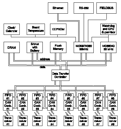
Each CAN channel is build using three building blocks:
A First-In-First-Out (FIFO) memory device.
A FPGA that connects the CAN controller to the FIFO and the 68360 microcontroller.
The CAN controller is accessible by the 68360 at the addresses as described in Memory Map of Each CAN Channel . Two additional addresses are defined to access the FIFO and the CAN Channel Configuration Register , which is internal to the FPGA.
Interrupt Active : When this read-only bit is set, at least one of the CAN controllers has its interrupt active.
DMA Enable : This read/write bit enables the DMA Controller of the FPGA to respond to receive interrupts from the CAN controller. When this bit is set, the microcontroller should read the received CAN messages from the FIFO device. When this bit is cleared, the microcontroller should read received CAN messages from the receive buffer of the CAN controller.
FIFO Empty : When this read-only bit is set, the FIFO device is empty.
FIFO Half Full : When this read-only bit is set, the FIFO device is half full.
Controller Interrupt Active : When this read-only bit is set, this CAN controller has its interrupt active.
The board status register is used to set and reset the CAN channel LEDs and to read back the FLEX status and the status of the CAN channels.
The board status register can be written and read back. Note that all bits are always written, so updating this register should always be a read-modify-write sequence. All written bits can be read back. The bits are used as follows:
|
See CAN Channel LEDs |
|||
|
See CAN Channel LEDs |
|||
|
See CAN Channel LEDs |
|||
|
See CAN Channel LEDs |
|||
|
See CAN Channel LEDs |
|||
|
See CAN Channel LEDs |
|||
|
See CAN Channel LEDs |
|||
|
See CAN Channel LEDs |
|||
The LED registers are initialized to `1's during reset.
The CAN status bits have different meaning when different options for the physical interfaces are chosen.
Although most of the functionality of the ethernet interface is managed by the communication processor of the 68360, some ethernet options can be set with the following bits.
|
In/Out |
||||
|
Auto Port Select Mode |
Manual Port Select Mode |
|||
The RS232 port has modem control lines which must be handled separately.
The AT25040 is a SPI compatible CMOS serial E2PROM. It can contain 4k (512 x 8) bit of information and provides write protection in software.
The SPI manager of the 68360 is used in the master mode providing clock and enable signals. The SPIMISO pin is then an input and is connected to the AT25040 serial data out pin.
The DS1305 RTC has an SPI interface and two additional interrupt outputs (open drain with external pull-up). The SPI will speed up the rate that the real time can be updated what can be an advantage when time stamping is needed for incoming CAN messages. The SPI is combined with the EEPROM SPI interface signals.
The Dallas DS1620 uses a three wire data transmission protocol. The RST and CLK inputs are connected to general purpose outputs, the DQ input/output pin of the DS1620 is connected to a three-state port pin and has a pull-up resistor.
The DS1620 has a temperature range of -55 to +125 degrees C in steps of 0.5 degrees C (9 bit value).
The Tcom signal (TTL output) is connected to a port C input. Port C inputs can generate interrupts on any change (low-to-high or high-to-low). The Tcom output changes when either Tlow or Thigh is exceeded. This gives an amount of hysteresis.
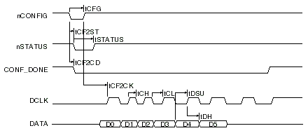
The Flex device is a SRAM based FPGA, which will loose its configuration during power down periods. After power up or when the Flex configuration needs to be updated during operation of the BI-0501, the in-circuit reconfiguration has to be executed.
A variety of indicator LEDs are available on the BI-0501.
Per CAN channel a bicolour LED is available. Each LED can be activated by writing two bits in the Board Status Register .
The ethernet interface has four LED indicators.
|
The interface indicates a good link integrity on the twisted pair port |
||
This is a bicolour LED for the processor status. The green LED is connected to general purpose I/O pin B16 with pull-up of the 68360 using an inverter-driver. After reset this pin will tri-state and the green LED will be turned off. The green LED will be lit when a zero is written to B16 . The RED led is connected via two inverter-drivers (the output of the first inverter goes to watch-dog circuit) to general purpose I/O pin B17 with pull-up to be sure that the red LED will be lit when a reset occurs. The red LED will be lit when a one is written to B17 .
A bicolour LED to verify whether 5Vdc is available. The green LED is connected to the high active RESET output of the power monitor DS1232, the red LED to the low active RESETN output of the DS1232. When power is applied the red LED will be active until the reset time-out of 250ms is passed. Then the green LED will be on. When power supply is below 4.75 V the red LED will be on.
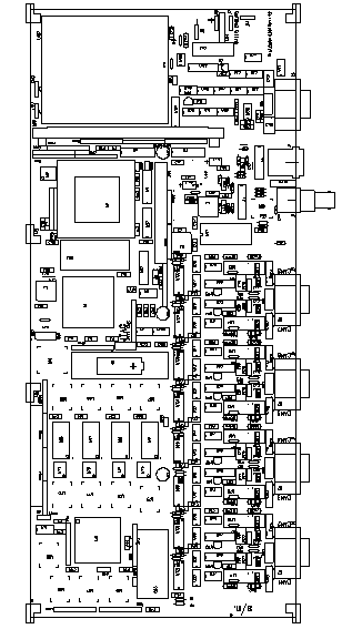
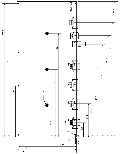
In this appendix the pinning is given of the CAN Connector , the 10Base-T Connector , the Thin Coax Connector , the RS-485 Connector , the RS-232 Connector and the Power Supply Connector .
The CAN connector is a 9 pin, male D type connector. This is the CAN interface port of the QUICC.
The 10Base-T connector is a 8 pin, RJ-45 connector. This is the twisted-pair Ethernet port of the QUICC.
The Thin Coax connector is a coax connector. It is the Thin Coax Ethernet port of the QUICC.
The RS-232 connector is a 9 pin, male D type connector. It is the RS-232 serial port of the QUICC.
The RS-485 connector is a 9 pin, female D type connector. It is the RS-485 serial port of the QUICC.
The Power Supply connector is a 3 pin connector. It is the Power Supply connector for the QUICC.
The Boundary Scan connector is a double-row, 10 pin, male connector. It provides access to the Boundary Scan signals of the BI-0501 for testing and programming purposes.
The BDM connector is a double-row, 10 pin, male connector. It provides the BDM signals of the QUICC, so that it can be controlled by an external BDM controller. Note that the BDM mode is not supported in the 68040 companion mode.
The following table gives the connection of the SIMM pins to the board signals.
|
MBAR registers in QUICC device and |
||
The following table gives the preferred address map for the BI-0501 chip select setup. Note that this preferred map is in no way dictated by the hardware and therefore a different address map may be selected. The upper two address bits should be zero, as described in MC68EC040 .
The eight CAN controllers occupy addresses that are 0x1000 apart.
The memory map of each CAN channel is identical. All registers are internal to the CAN controller except for the last two registers.